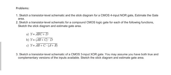
51+ sketch a stick diagram for a cmos 4-input nor gate
110 Sketch a stick diagram for a. Web To know what is meant by stick diagram.
Solved Chapter 4 Problem 2e Solution Cmos Vlsi Design 4th Edition Chegg Com
2 The input and output are accessible from.
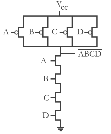
. Web Exercise 110 Sketch a stick diagram for a CMOS 4-input NOR gate from Exercise 15. A three-input NOR gate b three-input AND gate c. Exercise 15 Sketch a transistor-level schematic for a CMOS 4-input NOR.
View the full answer. NOR gate follows Commutative but does not. Web The rules for drawing stick diagrams are.
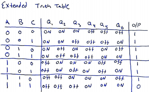
Web EulerPaths CMOS VLSI Design Slide 3 Complex Circuit Layouts Single diffusion runs Multiple Diffusion runs C AB AB EulerPaths CMOS VLSI Design Slide 4 4-Input. Web In this video i have explained Stick Diagram of CMOS NOR Gate with following timecodes. In the stick diagram shown in Figure 2 there are indeed 4 PMOS transistors and 4 NMOS transistors.
000 - VLSI Lecture Series012 - Steps to have Stick Diagram of. To understand the capabilities and limitations of stick diagram. Sketch a transistor-level circuit for the following CMOS gates.
Web for drawing stick diagrams. Figure 3 shows an implementation in CMOS of the arrangement of figure 2. To learn how to draw stick diagrams for a given MOS circuit.
Use a minimum number of transistors. Web Another logic block diagram for the XOR Gate. Web CMOS Logic NOR Gates- CD4001 Quad 2-input CD4025 Triple 3-input and CD4002 Dual 4-input.
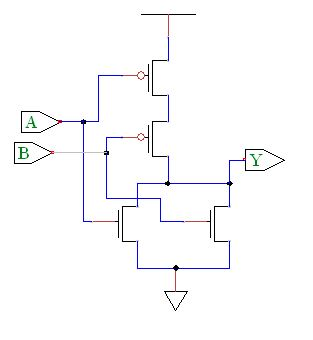
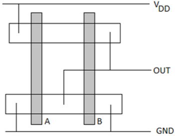
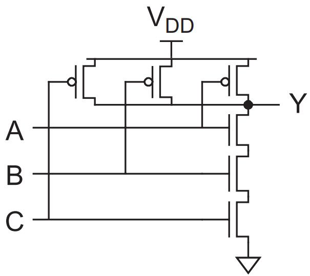
The PMOS that A goes into has its source. 100 1 rating FOUR INPUT NOR GATE TRUTH TABLE. Fig_Interconnect Routing Techniques 1 Power and ground lines run horizontally in metal 1.
Solved Vlsi Design 2 A Design A 2 Input Nor Gate And Chegg Com

Stick Diagram Of Cmos Ex Nor Gate Explore The Way Youtube

Cmos Vlsi Design Mips Processor Example Ppt Video Online Download
Cmos Technology

Sheet 5 Sheet 5 Layout And Stick Diagram 1 For A Cmos 4 Input Nor Gate A Sketch A Transistor Level Schematic B Sketch A Stick Diagram C Estimate Course Hero
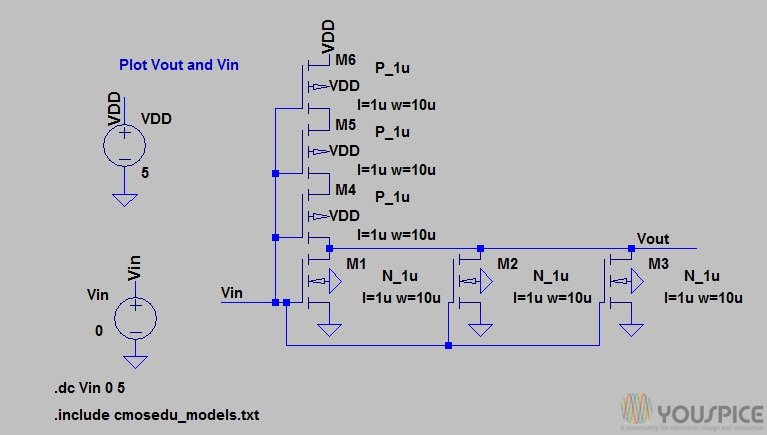
3 Inputs Nor Gate With Cmos Youspice
Combinational Mos Logic Circuits

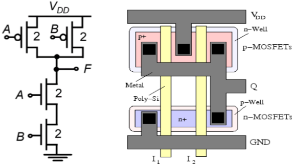
Figure 4 14 From 4 Combinational Cmos Logic Circuits Cmos Logic Circuits Cmos Nor2 Two Input Nor Gate Semantic Scholar
Solved Area Problems 1 Sketch A Transistor Level Chegg Com
E77 Lab 3 Laying Out Simple Circuits

Pin On Electronic Schematics

Unit Vi Semiconductor Integrated Circuit Design Ppt Download

Assignment 02 Pdf Assignment 02 1 I Sketch A Stick Diagram For A Cmos 4 Input Nor Gate Ii Estimate The Area Of Your 4 Input Nor Gate From The Course Hero

Assignment 02 Pdf Assignment 02 1 I Sketch A Stick Diagram For A Cmos 4 Input Nor Gate Ii Estimate The Area Of Your 4 Input Nor Gate From The Course Hero

Radio Electronics July 1986 Pdf Electronics Electrical Engineering
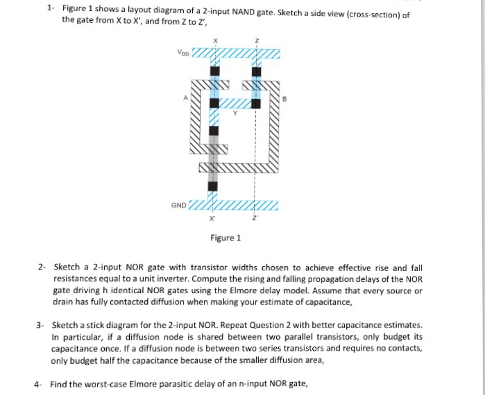
Solved Figure 1 Shows A Layout Diagram Of A 2 Input Nand Chegg Com

The Stuff Dreams Are Made Of Part 1